under the hood
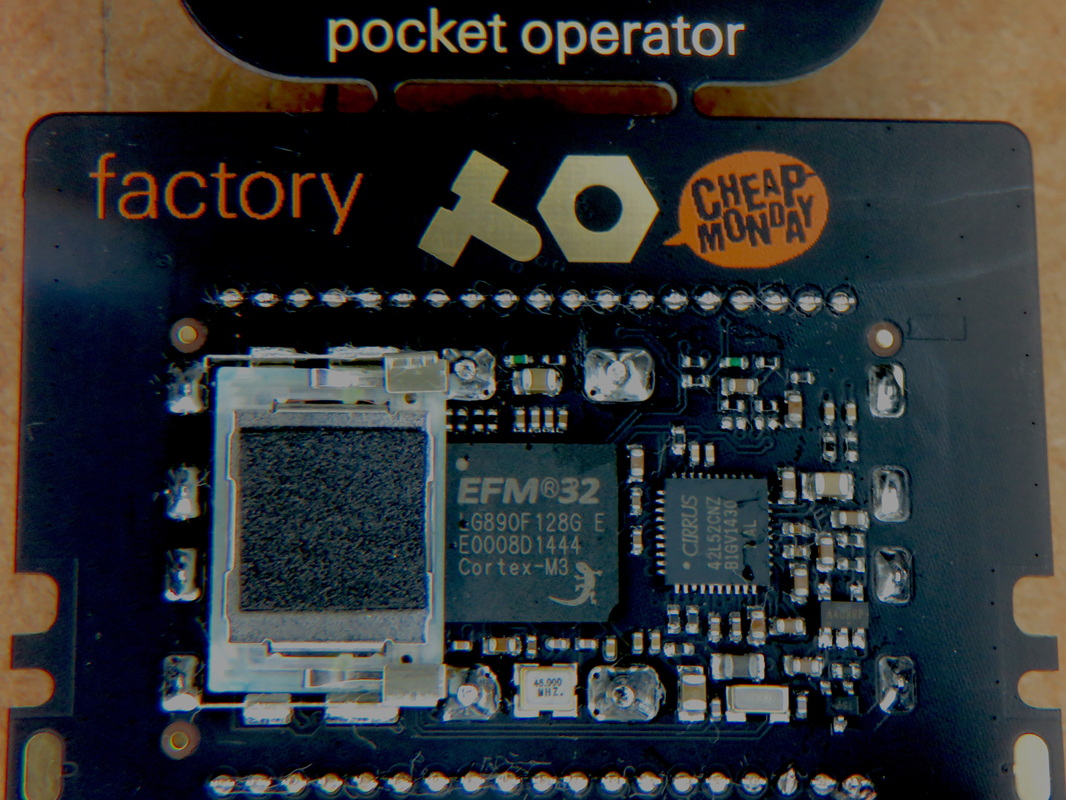
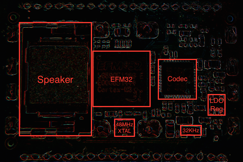
parts
Custom LCD display
EFM32LG890F128G (Cortex-M3, 48MHz, 32KB RAM, 128KB Flash)
CS42L52CNZ Cirrus Logic 24-bit Codec (stereo ADC and DAC)
48MHz main clock xtal
32KHz Epson watch xtal
2.5V LDO regulator w/ enable control
17x RED LEDs
23x tactile switches
2x 5K linear POTs
2x P2 stereo connectors
Knowles speaker
PARTS LOCATION
Exposed pads
There are some exposed pads at the back, most likely used at the factory for testing and flashing purposes:
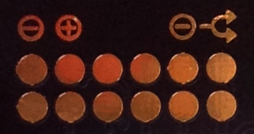
PADS MAPPING
 |
 |
|
|||
| GND | 3V | 2.5V | NC | GND | PLED |
| GND | RESET | SWCLK | SWDIO | SWO | 3V |
GND: Ground
3V: Connected to 3V battery thru protection
2.5V: Connected to codec VA and VD power source
NC: Not connected
PLED: Connected to Play LED anode
RESET: Connected to EFM32 reset pin
SWCLK: Connected to PF0 and 47R current limit resistor from Play LED
SWDIO: Connected to PF1 and to left channel in return line thru 4.7K resistor
SWO: Connected to PC15 and to left channel out return line thru 10K resistor
FLASHING INTERFACE
The firmware can be flashed using a J-Link interface available on the EFM32 Starter Kits from Silicon Labs, like the STK3600, STK3700 or STK3800.
FLASHING CABLE
FLASHING CABLE
| PO pad | J-Link connector |
|---|---|
| 3V | Pin 1 (VTARGET) |
| GND | Pins 18, 20 (Cable Detect/GND) |
| SWCLK | Pin 9 (TCK/SWCLK) |
| SWDIO | Pin 7 (TMS/SWDIO) |
| SWO | Pin 13 (TDO/SWO) |
| RESET | Pin 15 (#RESET) |
Notes:
- When flashing/debugging, it is better to insert dummy P2 plugs to both in/out connectors in order to disconnect the SWDIO and SWO signals from the audio return lines.
- The original firmware is locked. Once a new firmware is flashed, it is not possible to restore the original one!
MCU
The EFM32 is clocked by an external 48MHz crystal connected to PB13 (HFXTAL_P) and PB14 (HFXTAL_N). When powered down, after about 5 minutes of inactivity, it turns off that clock and the LED scanning, but not the codec. The 32KHz crystal connected to PB7 (LFXTAL_P) and PB8 (LFXTAL_N) is always running. Every half a second, there is a 7MHz burst for 120us at the CMU_OUT0 output, which may evidence that the MCU is running from the HFRCO at 14MHz during those periods. This continues even after 15 minutes of inactivity and is most likely related to the watch/alarm update logic.
The 128KB of internal flash memory is used for storing both the code and data. Since the debug interface was locked, it is not possible to access the flash contents. We may guess at the amount of memory used for storing the patterns on the PO-14/16 considering that:
For the PO-14/16, it would take 16*(16*(22+4*N)+4) bits to store all patterns, where N is the resolution of the pattern locks. That formula gives <2KB when N=8, which would fit in a single EFM32 flash page (2KB). The PO-12 most likely requires more memory because it supports multiple sounds per step.
- Sound and drum pattern locks appear at the output as linearly interpolated (4x Nb per step)
- 16 notes range for sound and drum (2x 4b per step)
- 16 punch-in effects (1x 4b per step)
- 16 styles (1x 4b per step)
- Note length for sound only (1x 4b per step)
- Note on/off for sound and drum (2x 1b per step)
- Selected pattern sound (1x 4b per pattern)
- 16 steps per pattern
- 16 patterns in total
For the PO-14/16, it would take 16*(16*(22+4*N)+4) bits to store all patterns, where N is the resolution of the pattern locks. That formula gives <2KB when N=8, which would fit in a single EFM32 flash page (2KB). The PO-12 most likely requires more memory because it supports multiple sounds per step.
LEDs
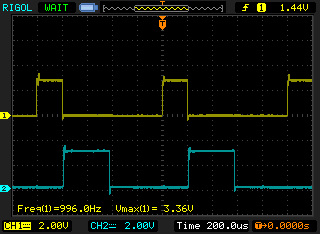
The 16 sequencer LEDs are arranged in a 4x4 matrix driven by eight GPIO outputs. Anodes are interconnected horizontally and cathodes vertically. Cathodes are connected to 47R current limit resistors. The scan rate is 1KHz, 200us high level per selected row (double period for the bottom one), with 42/16/3us low level pulses on each column for high/normal/low intensity, respectively. The Play LED is independently driven by PF0 with 1KHz, 16us high level pulses.
LEDS WAVEFORMS
LEDS WAVEFORMS
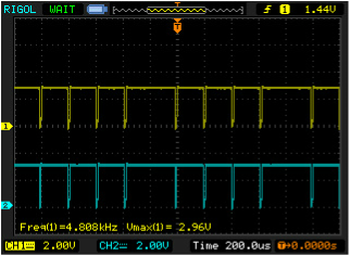
Two column signals with all LEDs lit.
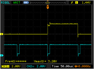
Row (above) and column (below) signals.
LEDS MAPPING |
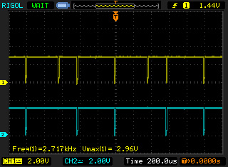
Two column signals with some LEDs off.
Third and fourth row scanning signals.
|
| EFM32 pin | PB1 (GPIO) | PA6 (GPIO) | PA3 (GPIO) | PA1 (GPIO) |
|---|---|---|---|---|
| PC0 (GPIO) | 1 | 2 | 3 | 4 |
| PA5 (GPIO) | 5 | 6 | 7 | 8 |
| PB3 (GPIO) | 9 | 10 | 11 | 12 |
| PB15 (GPIO) | 13 | 14 | 15 | 16 |
keys & pots
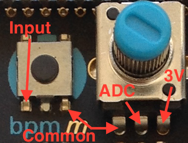
The 23 keys are connected to a common line, driven by PC14 (GPIO), and each to an independent GPIO input.
The POTs work as voltage dividers. The central tap is connected to the EFM32 ADC through a GPIO input and the other two pins are connected to the same common line as the keys and to 3V.
When the PO is active, the common line is set to 0V and each input is pulled-up to 3V. When the PO is sleeping, the common line is set to 3V and each input is pulled-down to 0V. That prevents the POTs from draining the battery while sleeping and also allows a high to low transition on PC14 to generate an interrupt and wake up the PO.
KEYS MAPPING
| sound PC1 (GPIO) |
pattern PD14 (GPIO) |
bpm PE1 (GPIO) |
left pot PD5 (ADC0_CH5) |
right pot PD4 (ADC0_CH4) |
| 1 PC2 (GPIO) |
2 PD15 (GPIO) |
3 PE0 (GPIO) |
4 PC7 (GPIO) |
keyoo PC12 (GPIO) |
| 5 PC3 (GPIO) |
6 PB11 (GPIO) |
7 PD8 (GPIO) |
8 PC10 (GPIO) |
style PC11 (GPIO) |
| 9 PC4 (GPIO) |
10 PD13 (GPIO) |
11 PB10 (GPIO) |
12 PC8 (GPIO) |
play PC9 (GPIO) |
| 13 PC5 (GPIO) |
14 PB12 (GPIO) |
15 PB9 (GPIO) |
16 PC6 (GPIO) |
write PE3 (GPIO) |
codec
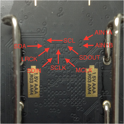
The codec VD and VA pins are powered by a 2.5V LDO regulator enabled by a logic high from PC13 (GPIO). VL and VP are powered by the protected 3V supply. MCLK is clocked at 24MHz. Samples are 16-bit (stereo). LRCK is 1.5MHz, which results in a 48KHz sample rate. The codec is powered down (and reset) after 15 minutes of inactivity.
The line in and line out plug presence is sensed by PF1 and PC15 respectively. These pins are configured as GPIO input with pull-up. A level high indicated that a plug is inserted.
CODEC MAPPING
The line in and line out plug presence is sensed by PF1 and PC15 respectively. These pins are configured as GPIO input with pull-up. A level high indicated that a plug is inserted.
CODEC MAPPING
| Codec pin | EFM32 pin |
|---|---|
| SPKR/HP | GND |
| RESET | PC13 (GPIO) |
| MCLK | PE2 (TIM3_CC2#1) |
| LRCK | PD3 (US1_CS#1) |
| SCLK | PD2 (US1_CLK#1) |
| SDIN | PD0 (US1_TX#1) |
| SDOUT | PD1 (US1_RX#1) |
| SDA | PD6 (I2C0_SDA#1) + 4.7K pull up to 3V |
| SCL | PD7 (I2C0_SCL#1) + 4.7K pull up to 3V |
| AD0 | GND |
| AIN1x | Line In |
CODEC VIAS
Some codec pins may be accessed from the back by exposing the board vias indicated below:
Some codec pins may be accessed from the back by exposing the board vias indicated below:
SPEAKER OUTPUT
The codec has a Class D speaker amplifier capable of driving a regular 4-8 Ohm speaker connected to the following pads at the back:
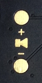
Note that the output is high-frequency a complementary PWM signal, i.e., the polarity does not matter.
CODEC CONFIGURATION
The I2C control port traffic shows that every write operation is immediately followed by a read (address = 95) on the same register to confirm that it was properly updated. These read operations are not depicted in the I2C dumps below.
Note that the original firmware will stop the code and turn on (full bright) key number 2 LED in case the codec initialisation fails.
Power up
94 // NAK is always received for this operation
94 05 a1 // auto-detection of speed mode, MCLK divide by 2
94 06 27 // slave mode, SCLK not inverted, I2S format up to 24-bit, DSP mode disabled, 16-bit audio word length
94 02 xx
// after 15 minutes of inactivity, xx=00: ADC charge pump, PGA and ADC channels and codec powered up
// before 15 minutes of inactivity, xx=9e: ADC charge pump, PGA and ADC channels powered down, codec powered up
// when powering up again before 15min of inactivity, the previous operations are omitted
94 26 f0 // PCM and ADC mix channel swap
94 08 81 // AIN1A input to ADCA
94 09 81 // AIN1B input to ADCB
94 12 00 // ALCA soft ramp disabled
94 13 00 // ALCB soft ramp disabled
94 16 0c // ADCA volume = 12dB
94 17 0c // ADCB volume = 12 dB
94 20 f0 // master volume A = -6dB
94 21 f0 // master volume B = -6dB
94 27 04 // limiter maximum and cushion thresholds = 0dB, soft ramp override on, zero cross override off
94 0f 02 // headphone and speaker mute disabled, volume A/B independent, speaker mono, 50/50 mute disabled
94 1f 8f // treble gain = 0 dB, bass gain = -10.5dB
94 1e 06 // beep off, tone control disabled
94 04 0a // headphone on, speaker on
94 0f 02 // headphone and speaker mute disabled, volume A/B independent, speaker mono, 50/50 mute disabled
Power down (5min)
94 04 ff // power off headphone and speaker channels
94 02 9f // power down PGA, ADC and codec
Play note (sequencer stopped)
94 0f 02 // headphone and speaker mute disabled, volume A/B independent, speaker mono, 50/50 mute disabled
94 0e 03 // passthrough mute, freeze and de-emphasis disabled, volume soft ramp and zero cross enabled
94 0f f2 // headphone and speaker mute enabled, volume A/B independent, speaker mono, 50/50 mute disabled
94 0e 00 // passthrough from PGA to hp/line out disabled, passthrough mute, freeze and de-emphasis disabled
94 02 9e // ADC charge pump, PGA and ADC channels powered down, codec powered up
Start sequencer
94 0f 02 // headphone and speaker mute disabled, volume A/B independent, speaker mono, 50/50 mute disabled
94 0e 03
// passthrough from PGA to hp/line out, passthrough mute, freeze and de-emphasis disabled
// volume soft ramp and zero cross enabled
Stop sequencer
94 0f f2 // headphone and speaker mute disabled, volume A/B independent, speaker mono, 50/50 mute disabled
94 0e 00
// pass through from PGA to hp/line out, passthrough mute, freeze and de-emphasis disabled
// volume soft ramp and zero cross disabled
94 02 9e // ADC charge pump, PGA and ADC channels powered down, codec powered up
Set Volume
94 20 xx // set volume A
94 21 xx // set volume B
// volume 1-16 when driving the speaker: 38, c4, d8, e8, f0, f4, f8, fc, 00, 04, 08, 0c, 10, 14, 16, 18
// volume 1-16 when line out is connected: 38, 9c, b0, c4, d8, e0, e8, f0, f8, fc, 00, 04, 08, 0c, 10, 18
Out connected
94 20 xx // set volume A
94 21 xx // set volume B
94 04 aa // headphone and speaker channels on
94 0f f2 // headphone and speaker mute enabled, volume A/B independent, speaker mono, 50/50 mute disabled
94 04 af // headphone channel on, speaker channels off
94 28 3f // limiter off
94 20 xx // set volume A
94 21 xx // set volume A
94 1f 80 // treble gain = 0dB, bass gain = 12dB
Out disconnected
94 04 ff // headphone and speaker channels off
94 20 xx // set volume A
94 21 xx // set volume B
94 27 04 // limiter maximum and cushion thresholds = 0dB, soft ramp override on, zero cross override off
94 0f f2 // headphone and speaker mute enabled, volume A/B independent, speaker mono, 50/50 mute disabled
94 1f 8f // treble gain = 0dB, bass gain = -10.5dB
94 1e 06 // beep off, tone control disabled
94 04 fa // headphone channel off, speaker channels on
94 0f c2 // headphone mute enabled, speaker mute disabled
In connected
94 0f 02 // headphone and speaker mute disabled, volume A/B independent, speaker mono, 50/50 mute disabled
94 0e 03 // passthrough mute, freeze and de-emphasis disabled, volume soft ramp and zero cross enabled
94 2c 00 // ALC max threshold = 0dB, ALC min threshold = 0dB
94 2a c0 // ALC enabled, fastest attack
94 02 00 // ADC charge pump, PGA and ADC channels and codec powered up
94 0f f2 // headphone and speaker mute enabled, volume A/B independent, speaker mono, 50/50 mute disabled
94 0e 00 // passthrough from PGA to hp/line out disabled, passthrough mute, freeze and de-emphasis disabled
94 02 9e // ADC charge pump, PGA and ADC channels powered down, codec powered up
94 2c 3c // ALC max threshold = -3dB, ALC min threshold = -30dB
In disconnected
94 02 9e // ADC charge pump, PGA and ADC channels powered down, codec powered up
94 0f f2 // headphone and speaker mute enabled, volume A/B independent, speaker mono, 50/50 mute disabled
94 0e 00 // passthrough from PGA to hp/line out disabled, passthrough mute, freeze and de-emphasis disabled
94 02 9e // ADC charge pump, PGA and ADC channels powered down, codec powered up
SY0 mode
94 2a 00 // ALC disabled
94 20 xx // set volume A
94 21 xx // set volume B
92 2a c0 // ALC enabled, fastest attack
SY1 mode
94 2a c0 // ALC enabled, fastest attack
94 20 xx // set volume A
94 21 00 // set volume B = 0dB
SY2 mode
94 2a 00 // ALC disabled
94 20 xx // set volume A
94 21 xx // set volume B
SY3 mode
94 2a 00 // ALC disabled
94 20 xx // set volume A
94 21 xx // set volume B
SY4 mode
94 2a 80 // ALC channel B enabled, ALC channel B fastest attack, ALC channel A disabled
94 20 xx // set volume A
94 21 xx // set volume B
SY5 mode
94 2a 80 // ALC channel B enabled, ALC channel B fastest attack, ALC channel A disabled
94 20 xx // set volume A
94 21 xx // set volume B
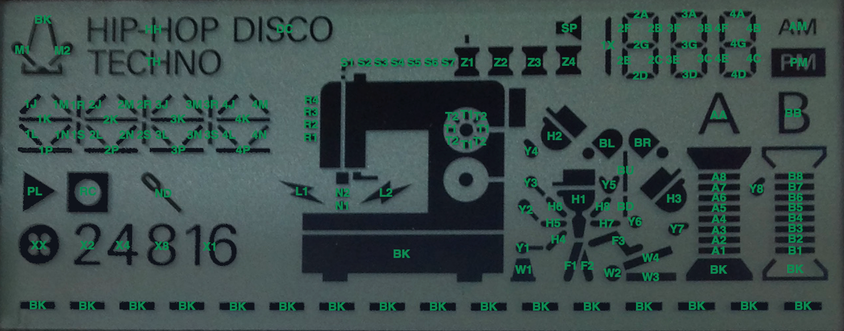
display
The display is multiplexed. Common pins are 1-4, segment pins are 5-38. The LCD driver is configured to 32Hz refresh rate, 1/3 bias quadruplex multiplexing (8x 4ms), low power waveform, 3.28Vpp. The voltage boost capacitors are connected to PA12 (LCD_BCAP_P), PA13 (LCD_BCAP_N) and PA14 (LCD_BEXT). Segments 14, 18, 19, 20 and 33 are not used.
DISPLAY MAPPING
DISPLAY MAPPING
|
|
PO-16 DISPLAY
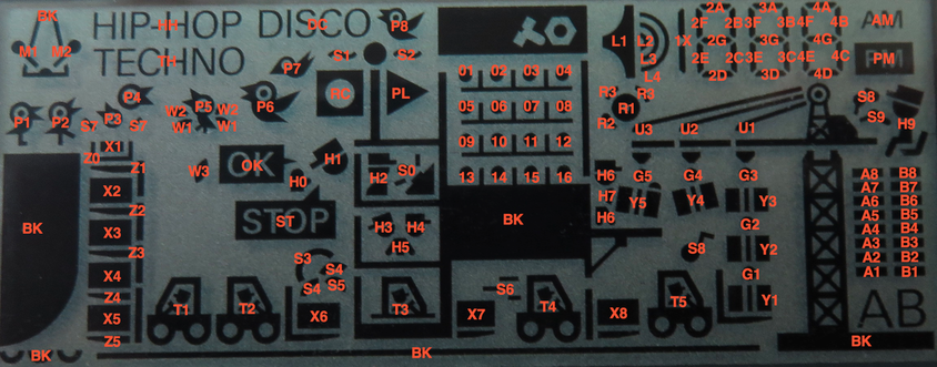
Pin 1
| PIN | 01 | 02 | 03 | 04 | 05 | 06 | 07 | 08 | 09 | 10 | 11 | 12 | 13 | 14 | 15 | 16 | 17 | 18 | 19 |
|---|---|---|---|---|---|---|---|---|---|---|---|---|---|---|---|---|---|---|---|
| C0 | C0 | -- | -- | -- | Z1 | X4 | Z4 | T1 | T2 | S5 | T4 | X8 | Y4 | T5 | Y1 | A8 | A1 | B1 | B8 |
| C1 | -- | C1 | -- | -- | Z0 | Z4 | X3 | OK | ST | S4 | S6 | Y5 | G4 | S8 | G1 | A7 | A2 | B2 | B7 |
| C2 | -- | -- | C2 | -- | X1 | X5 | Z2 | H1 | H0 | S3 | X7 | H7 | G5 | Y3 | Y2 | A6 | A3 | B3 | B6 |
| C3 | -- | -- | -- | C3 | H2 | Z5 | X2 | H4 | H3 | H5 | T3 | H6 | U1 | G3 | G2 | A5 | A4 | B4 | B5 |
| PIN | 20 | 21 | 22 | 23 | 24 | 25 | 26 | 27 | 28 | 29 | 30 | 31 | 32 | 33 | 34 | 35 | 36 | 37 | 38 |
|---|---|---|---|---|---|---|---|---|---|---|---|---|---|---|---|---|---|---|---|
| C0 | AM | 4A | 4F | 3A | 3F | 2A | 2F | L1 | R3 | 13 | 09 | 01 | 05 | P8 | P7 | P6 | HH | P1 | ? |
| C1 | PM | 4B | 4G | 3B | 3G | 2B | 2G | L2 | R1 | 14 | 10 | 02 | 06 | S2 | S1 | W1 | TH | P2 | M2 |
| C2 | S8 | 4C | 4E | 3C | 3E | 2C | 2E | L3 | R2 | 15 | 11 | 03 | 07 | DC | RC | W2 | P4 | S7 | M1 |
| C3 | H9 | 4D | S9 | 3D | U3 | 2D | 1X | L4 | U2 | 16 | 12 | 04 | 08 | PL | S0 | P5 | P3 | W3 | BK |
PO-14 DISPLAY
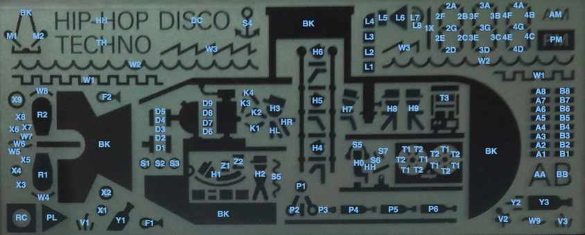
Pin 1
| PIN | 01 | 02 | 03 | 04 | 05 | 06 | 07 | 08 | 09 | 10 | 11 | 12 | 13 | 14 | 15 | 16 | 17 | 18 | 19 |
|---|---|---|---|---|---|---|---|---|---|---|---|---|---|---|---|---|---|---|---|
| C0 | C0 | -- | -- | -- | X9 | H2 | K1 | HL | P1 | P6 | H7 | S5 | H0 | Y3 | S5 | B4 | A4 | A5 | B5 |
| C1 | -- | C1 | -- | -- | W8 | Z2 | K2 | HR | P2 | P5 | H8 | S6 | HH | V3 | BB | B3 | A3 | A6 | B6 |
| C2 | -- | -- | C2 | -- | R2 | Z1 | K3 | H3 | P3 | P4 | H9 | W9 | ? | W9 | AA | B2 | A2 | A7 | B7 |
| C3 | -- | -- | -- | C3 | BK | H1 | K4 | H6 | H5 | H4 | T3 | T1 | T2 | V2 | Y2 | B1 | A1 | A8 | B8 |
| PIN | 20 | 21 | 22 | 23 | 24 | 25 | 26 | 27 | 28 | 29 | 30 | 31 | 32 | 33 | 34 | 35 | 36 | 37 | 38 |
|---|---|---|---|---|---|---|---|---|---|---|---|---|---|---|---|---|---|---|---|
| C0 | 4B | 4A | 3B | 3A | 2B | 2A | L5 | L4 | HH | W3 | M2 | X8 | W5 | X5 | RC | F1 | D9 | D2 | S1 |
| C1 | 4G | 4F | 3G | 3F | 2G | 2F | L6 | L3 | DC | W2 | ? | X7 | W6 | X4 | PL | Y1 | D8 | D3 | S2 |
| C2 | 4C | 4E | 3C | 3E | 2C | 2E | L7 | L2 | S4 | W1 | ? | X6 | W7 | X3 | V1 | X1 | D7 | D4 | S3 |
| C3 | AM | 4D | PM | 3D | 1X | 2D | L8 | L1 | TH | F2 | ? | M1 | ? | R1 | W4 | X2 | D6 | D5 | D1 |
PO-12 DISPLAY
Pin 1
| PIN | 01 | 02 | 03 | 04 | 05 | 06 | 07 | 08 | 09 | 10 | 11 | 12 | 13 | 14 | 15 | 16 | 17 | 18 | 19 |
|---|---|---|---|---|---|---|---|---|---|---|---|---|---|---|---|---|---|---|---|
| C0 | C0 | -- | -- | -- | X8 | R1 | L2 | N2 | N1 | L1 | T2 | T1 | Y4 | ? | BL | BU | BR | A8 | A7 |
| C1 | -- | C1 | -- | -- | 2R | 3J | 3M | 3R | 4J | 4M | Y2 | Y3 | H6 | H8 | Y5 | BD | H3 | A6 | A5 |
| C2 | -- | -- | C2 | -- | 2S | 3K | 3N | 3S | 4K | 4N | Y1 | H5 | H1 | H7 | F3 | Y6 | Y7 | A4 | A3 |
| C3 | -- | -- | -- | C3 | ND | 3L | 3P | X1 | 4L | 4P | W1 | H4 | F1 | F2 | W2 | W4 | W3 | A2 | A1 |
| PIN | 20 | 21 | 22 | 23 | 24 | 25 | 26 | 27 | 28 | 29 | 30 | 31 | 32 | 33 | 34 | 35 | 36 | 37 | 38 |
|---|---|---|---|---|---|---|---|---|---|---|---|---|---|---|---|---|---|---|---|
| C0 | B7 | B8 | Y8 | 4D | AA | 3D | H2 | 2D | 1X | Z2 | BK | S2 | S1 | DC | TH | HH | M2 | M1 | PL |
| C1 | B5 | B6 | BB | 4C | 4E | 3C | 3E | 2C | 2E | Z3 | Z1 | S3 | R4 | 2M | 2J | 1R | 1M | 1J | XX |
| C2 | B3 | B4 | PM | 4B | 4G | 3B | 3G | 2B | 2G | Z4 | S7 | S4 | R3 | 2N | 2K | 1S | 1N | 1K | X2 |
| C3 | B1 | B2 | AM | 4A | 4F | 3A | 3F | 2A | 2F | SP | S6 | S5 | R2 | 2P | 2L | RC | 1P | 1L | X4 |
Notes:
- C0-C3 are the common pins.
- BK is mapped to all background symbols.
The names have been changed to protect the innocent...
